CSAR 62 for thick films
Intensive plasma etching applications for the manufacture of deep etching structures with a high aspect ratio require etch-resistant resists and higher layer thicknesses, which however place particular demands on resolution and contrast.
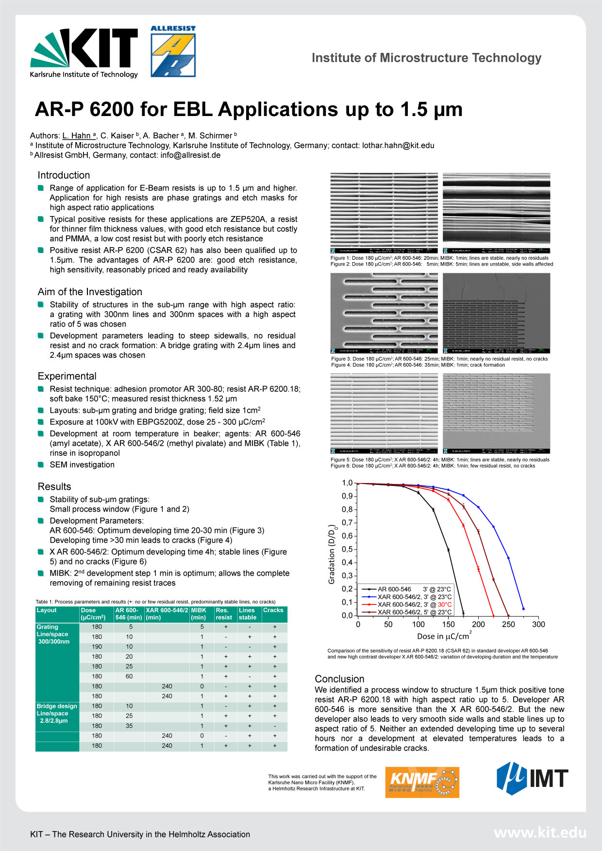
Layers with a thickness of 1.5 μm were produced using AR-P 6200.18, thick. As shown by investigations at the KIT (IMT, Dr. Lothar Hahn), allows this layer thickness to generate very regular trenches with a width of 300 nm at a period of 300 nm (see Fig. 1).
The high contrast of 5 is made possible by the use of our developer AR 600-546. Briefly rinsing with MIBK yields a residue-free development.
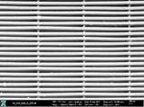
Fig. 1: Dose 180 µC/cm2 at 100 kV; AR 600-546: 20 min, MIBK: 1 min; stable, highly regular line structure
A decisive parameter is the development process: Longer development times of > 30 minutes are unfavourable since stress cracking can occur in the relatively thick layers (Fig. 2).

Fig. 2: Dose 180 µC/cm2 at 100 kV; AR 600-546: 35 min, MIBK: 1 min; formation of stress cracks
Also a new developer was tested within the scope of these. Developer X AR 600-546/2 also develops with very high contrast, is however less sensitive than the standard developer AR 600-546.
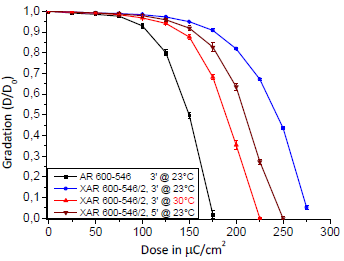
Fig. 3: Gradation of AR-P 6200.18 in AR 600-546 and new developer X AR 600-546/2 in comparison
Increasing the developer temperature to 30 °C causes a considerable increase in the sensitivity without reducing the contrast significantly. Furthermore, also extending the development time increases the sensitivity. 1.5 μm layers of CSAR 62 could be developed without any interfering cracks with X AR 600-546/2.
Fig. 4: Dose 180 µC/cm2 at 100 kV; X AR 600-546/2: 4 h, MIBK: 1 min; stable, highly regular residue-free developed line structure without cracks