Interference lithography is a less frequently used method for patterning. The basic principle is the same as in interferometry or also in holography. The superposition of two or more coherent light waves creates a periodic interference pattern consisting of a series of intensity maxima and minima (superposition or extinction), which can then be transferred into light-sensitive films (photoresists). In the case of two-beam interference, a fringe-to-fringe spacing or period of (λ/2)/sin(θ/2) results, whereby θ is the angle between the waves superimposed on each other and λ the wavelength of light used. The smallest possible period is determined by the wavelength and given as λ/2. If laser light is used for interference lithography, periodic structures with minimum sizes down to about 100 nm can be produced. Since whole wafers can be exposed at once, the throughput is high and the process accordingly very cost-efficient. Disadvantageously however is that this method is limited to one- or two-dimensional periodic grids. Interference lithography is nevertheless the method of choice for the fabrication of submicron gratings, since no other process enables such high-quality lattices on large surfaces. [Reference: Dissertation “Interferenzlithographisch strukturierte Oberflächen für lichtemittierende Bauelemente“; Dipl.-Phys. Ulf Geyer; University of Karlsruhe (TH), Department of Electrical Engineering and Information Technology; 2009]
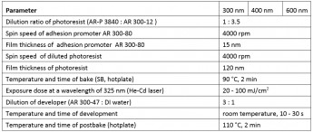
At the Chinese Academy of Sciences (CAS), sub-µm gratings with a high resolution of up to 70 nm (line width) could be realized with AR-P 3840. Excerpt from a report by Dai Longgui, Ding Peng and Prof. Chen Hong (Renewable Energy Laboratory, Institute of Physics, IOP): “Using laser interference lithography, we produced sub-µm photoresist gratings in silicon. We easily managed to generate various sub-µm periods of 200 to 800 nm. The different gratings could be obtained by varying the interference angle, the exposure dose and the development conditions. Details of the process parameters are presented in the following table:”
Table 1: Process parameters of laser interference lithography with positive resist AR-P 3840
Fig. 1: Experimental setup for laser interference lithography
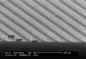
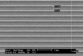
The following figures demonstrate a selection of the highly regular lattice structures which can be obtained. At a film thickness of 111 nm, the period is 181 nm with a line width of about 100 nm or a period of 323 nm with a line width of only 72 nm!
Fig. 2: Photoresist grid with 180-nm period
Fig. 3: 323-nm period with 72-nm line width
Also negative photoresists are suitable for interference lithography. In this case, resist which were crosslinked via the mechanism of chemical amplification (CAR) yield particularly smooth edges and show no distinct first interference minimum in the developed structures. By using a special version of our standard resist AR-N 4340 (SX AR-N 4340/8), interference lithography could also successfully be carried out under white light conditions (MLU Halle; Center for Material Science, Dr. Fuhrmann):
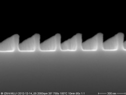
Fig. 4: SX AR-N 4340/8 line structures with 57 nm line diameter at a film thickness of 191 nm; further parameters: 232 nm period, angle: 35°, exposure for 750 s at 266 nm with an output power of about 0.01 mW/cm2, PEB for 10 minutes at 100 °C; development: 90 s with AR 300-47 (diluted 1:1).
Beautiful and even line structures with vertical walls were produced in this case. At a period of 232 nm, an excellent resolution of only 57 nm was realised!
Also negative resists which do not crosslink via a CAR-mechanism can be used for laser interference lithography. Our negative resist AR-N 4240 is for example used on a standard basis for lift-off processes. The undercut resulting from standing waves is desired in this case, but nevertheless limits the resolution.
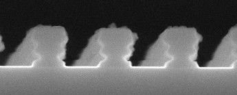
Fig. 5: Typical edge profile of AR-N 4240 (MLU Halle, dilution 1: 2 with AR 300-12, 4000 rpm, SB 85 °C, exposure: 160 s with about 16-20 mJ at 266 nm, PEB 30 min at 85 °C; development: 30 s with AR 300-475).
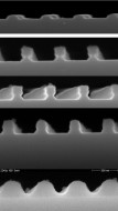
The edge shape can be selectively adjusted by varying the PEB temperature.
Fig. 6: Processed structures from top to bottom: PEB at 90, 95, 100, 105 and 110 °C, respectively.
In order to reduce the processing times, the PEB time was shortened to 5 minutes each while the temperature was simultaneously increased in 5 °C-steps. At a PEB of 90 °C, stripes deriving from the first minimum dissolve. Between 95 and 100 °C, resist profiles are comparable to those obtained under standard conditions. At 105 °C, the narrowing at the first minimum disappears, and at 110 °C, the structures could no longer be developed. Optimal turned out to be a PEB temperature of 105 °C. The undercut disappears completely at this temperature, which allows for smaller periods and makes AR-N 4240 suitable for reactive iron etching (RIE) processes.
Further reference (MLU): Johannes de Boor, Nadine Geyer, Jörg V. Witteman, Ulrich Gösele and Volker Schmidt: „Sub-100 nm silicon nanowires by laser interference lithography and metal-assisted etching“ Nanotechnology 21 (2010) 095302 (5pp); doi: 10.1088 / 0957-4484 / 21/9/095302
