PPA layers are sensitive to light and can thus be structured directly by photolithography. Irradiation with light of wavelengths < 300 nm (Hg vapour lamp) results in a cleavage of the polymer chains and the formation of volatile components that partly begin to evaporate even at room temperature. This dry (developer-free) development process is completed by heating the exposed substrates to about 100 – 120 °C. Photosensitivity can generally be increased by adding acid formers (PAGs). Recommend for stripping/removal is either an etching with plasma or heating the substrate to about 200 °C, which results in a residue-free evaporation of the PPA.
The addition of PAGs (photo acid generators) significantly increases the sensitivity. During exposure, acid is released in situ which decomposes the PPA layer during the subsequent PEB step (and sometimes even already at room temperature). The choice of suitable PAGs and the optimal PAG concentration are thus crucial parameters for this process. Numerous PAGs assessed in this respect lead only to an incomplete development. In the case of variant 8100/3, overexposure even results in higher layer thicknesses which are caused by UV-induced cross-linking reactions:
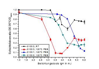
Fig. 1: Layer thickness as a function of the exposure dose, no complete development possible
PPA variants 8100/2 and 8100/3 are considerably more sensitive than 8100/1 (pure PPA without additives), due to the addition of PAGs. However, a 100 % positive thermal development at 120 °C could not be observed. In the case of 8100/3, development occurs already partly at room temperature, but this development is incomplete without subsequent PEB.
The new samples 8100/4,5,6, and 7 contain an acid generator that enables complete thermal development already at a PEB of 98 °C which is well below the decomposition temperature of PPA. Exposure succeeds only at wavelengths < 300 nm. PPA layers with different PAGs are storage-stable for at least a few days.
The optimised formulations (variation of PAG concentration) allow (almost) complete thermal development (up to the detection limit of layers with a thickness of a few nanometres). A complete development can be achieved with a short plasma etching step.
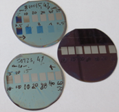
Fig. 2: Complete development of irradiated squares with new PAG
Decisive influencing factors are:
- PAG concentration (too little results in an incomplete development; too much narrows the process window)
- Exposure dose (and wavelength)
- Temperature and duration of the PEB
- Time interval between exposure and PEB (the observed sensitivities are higher if the PEB is carried out immediately after exposure)
- Film thickness (thinner films are more sensitive)!
Overview Other Resists