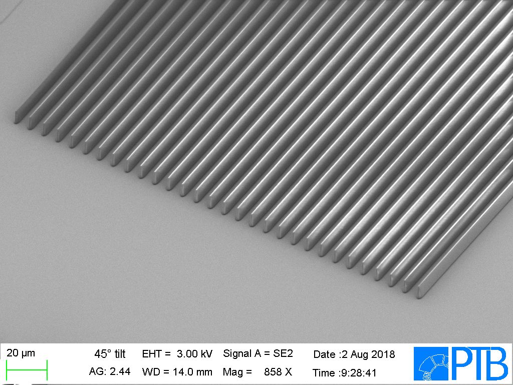
Layer thicknesses of more than 5 μm are rarely required for electron beam lithography, and consequently only isolated attempts have been made to pattern PMMA layers up to a layer thickness of 20 μm by electron beam exposure. The PMMA e-beam resist AR-P 6510 is suitable for this purpose, but special developers (AR 600-51) and stoppers (AR 600-61) are needed for the subsequent development. If conventional MIBK/isopropanol developers are used, the layer will in most cases crack during the development step.
We now succeeded in finding a remarkable solution for high-layer e-beam structuring. The negative resist CAR 44 (AR-N 4400-10) was coated to yield a layer with a height of 9.5 μm, dried, and irradiated.
At a dose of about 40 μC/cm² (100 kV), 2 μm wide lines were written, cross-linked at 105 °C and developed with developer AR 300-26.

2 µm lines generated by e-beam lithography in a layer with a thickness of 9.5 µm
Even layers with higher film thicknesses can be structured. CAR 44 is thus also suitable as electron beam resists for this kind of applications.
