1. Brief History of Imaging Techniques
Imaging for microelectronics is rooted in both printing technology and photography. Already in the 1st century AD, the Diamond Sutra (“The diamond that cuts through illusion”) was produced in China with wood block printing. Each character was carved mirror-inverted into a wooden panel, the shapes then rubbed in with colour and pressed onto paper. By these means, a text could also be reproduced. A revolutionary improvement was Gutenberg’s letterpress in 1450. Movable metallic letters placed in a printing frame allowed for the first time to produce many copies of a text.
The first imaging technique involving light was developed about 1826 by Joseph Nicephore Niépce who invented the first real photolithography method [1, 2]. The Greek words photo (-> light), litho (-> stone) and graphic (-> writing) exactly describe this process. Niépce used a special form of bitumen which he coated onto a tin plate and exposed with a “camera obscura” for eight hours. Bitumen hardens under the influence of light, and the non-hardened areas were subsequently washed out with lavender oil.

Fig.1 First photograph by Niépce 1826 (retouched reproduction, 1952)1)
The basics of modern photolithography were laid in 1935 when Louis Minsk developed the first negative photoresist based on cyclic cis-polyisoprene (“cyclised rubber”) [3, 4]. He dissolved the polymers in organic solvents and added light-sensitive bisazides. If such layers are exposed using a template, the exposed areas are cross-linked. The layer was then treated with a solvent mixture whereby the exposed patterns remained and the unexposed were washed away. An example of a commercial resist of this kind is the Kodak Thin Film Resist (KTFR) which was widely in use from 1957 up into the 1990s.
In 1940, Oskar Sues created a positive photoresist process based on naphthoquinonediazide which is still today considered the “workhorse” of photolithography (see section 4 for a description of the Sues reaction) [5].
Photography and photolithography have a lot in common; both methods can be used to produce high-precision images and in both cases, images (patterns) are projected onto a light-sensitive layer by cameras or mask aligners. The exposure to light induces chemical changes that can be made visible by a development of the layer. The important difference in the methods is the preservation of the layer. While in photography layers remain intact and only the transparency in the desired areas changes, parts of the layer are completely removed in photolithography and the substrate surface is exposed.
In the middle of the 20th century thus a negative and a positive photoresist were available which also initiated the development of integrated circuits (transistors, microchips). Since then, dozens of resists have been developed which allow for a wide variety of applications.
2. Industrial Applications of Photoresists
While photoresists were primarily used in the manufacture of printed circuit boards [6], printing plates [7], transistors [8] and, beginning, also of integrated circuits in the 1970s and 1980s, resists are today applied in a wide variety of fields of the electronics industry. The focus is set by microelectronics and semiconductor production which accounts for almost 50 % of the resists used worldwide [9]. The circuit board industry consumes about 30 %; the remaining 20 % are spread across different industrial areas such as optoelectronics, sensor technology, electroplating, optical industry, micro-electro-mechanical systems (MEMS), nanotechnology, nanoimprinting, TFT displays (thin-film transistors) and photomask production [10]. Special processes and technologies for most applications were developed, opening up an almost inexhaustible field of industrial uses. And, not to forget, a significant amount of resists are also required for research purposes.
Probably everyone interested in microelectronics knows Moore’s Law [11]. Gordon Moore observed in 1965 that the complexity in dense integrated circuits doubles approximately every 18 months with minimal component costs (Fig. 2). With the term “complexity”, Gordon meant in this context the number of transistors that could be placed on one integrated circuit chip.

Fig. 2 Moore’s Law: In the period under consideration, the number of transistors doubles approximately every 18 months 2)
This increasing complexity proved to be the ultimate driving force in the development of photolithography. Only through ever smaller resist structures became it possible to accommodate more and more transistors on a chip. It is nevertheless discussed controversially if the physically feasible limits have not been reached meanwhile [12]. The smallest, currently realisable structures are 2.5 nm (see 4.1.5.). Since the bond lengths of molecules are in a range of about 0.2 nm, the scope is slowly becoming narrow – unless completely new solutions are developed (e.g. quarks [13, 14], graphs [15], or others).
The multitude of conceivable applications explains the wide range of technology-specific lithography processes today, but all of them are still based on the photolithography standard process, which is in detail described in the following section.
3. Standard Processes in Photolithography
- Adhesion promotion
- Resist coating
- Softbake
- Alignment
- Exposure
- Post-exposure bake (PEB, optional)
- Development
- Measurement and inspection (optional)
- Hard bake (optional)
- Technological steps
- Removal (Stripping)
This process is often repeated several times during the manufacture of an integrated circuit (IC). An IC typically contains a combination of numerous electrically connected electronic semiconductor components, transistors, diodes and/or additional active and passive components, the production of which may require up to 100 process steps in complex circuits. Fig.3 visualises the large number of involved steps for the construction of a simple transistor. References [16] and [17] are recommended for further information on the lithographic process.

Fig. 3 Construction of a simple transistor and required process steps 3)
3.1. Adhesion Promotion:
Each resist is characterised by its own polarity and surface tension. Since the surfaces of substrates also differ, a treatment of the wafer with an adhesion promoter is in most cases highly recommended. Otherwise, wafers may only be insufficiently and/or not uniformly coated by the resist.
In most coating procedures, a pre-treatment of the substrates (mostly silicone, but also gallium arsenide, metals, glass etc.) is required. Even brand-new silicon wafers carry OH groups on their surface, rendering the surface hydrophilic (Fig. 4). Since most resists are hydrophobic, the hydrophilic properties of the wafers must be eliminated. This is often done by vapour deposition of HMDS (hexamethyldisilazane) at 160 °C.

Fig. 4 Mode of HMDS action to promote adhesion of the resist coating 4)
HMDS reacts with the OH groups of the silicon wafer and creates a hydrophobic surface (Fig. 4) which facilitates resists adhesion. Alternatively, also a short dip in dilute hydrofluoric acid removes the hydrophilic groups on the silicone surface reliably. In this case however, the wafer must be processed quickly since otherwise new OH groups will form on the surface due to the air humidity.
The easiest way to achieve a sufficiently high adhesion promotion is to heat the wafers at 200 °C which removes the mono-molecular water layer. In the cleaning of pre-used wafers, acetone should never be used in the final step. Acetone evaporates quickly and cools the wafer surface, thus causing water to condense on the surface which renders it hydrophilic again. Alternatives for adhesion promotion offer TI-Prime {5} and AR 300-80 {1}. Both adhesion promoters are not evaporated, but spun onto the wafer and tempered, which simplifies the technology.
3.2. Resist Coating:
The by far most frequently used coating method is spin coating. A small amount of the fluid resist (1 – 10 ml) is dispensed on the wafer. When the wafer rotates, the resist spins off the edges of the substrate. The solvent evaporates and layer thicknesses of typically 0.1 – 5 µm result, but thickness values of up to several hundred µm are possible. Meanwhile, spin coating is used to coat 300 mm (12 inch) wafers with an accuracy of 1 – 2 nm thickness.
Spray coating is primarily used for the coating of high topography substrate surfaces with e.g. deep etching trenches (Fig. 5). A spray coater (Fig. 5a) disperses a fast-drying resist through a nozzle system into fine droplets (⦸ 5 – 10 µm) which are subsequently deposited on the substrate. The “art” of coating is the interplay between a quick drying and a sufficiently high spreading of the wet resist on the surface. If resists dry too fast, the resulting surface will be rough or the droplets dry already in the air and form pellets on the surface. If the resist on the other hand remains liquid for too long, it will retract from the edges due to the surface tension (see Fig. 5c). Spray coating can also be successfully used for irregularly shaped or spherical substrates.

Fig. 5a Spray coater of the company EVG 5a)

Fig. 5b 200 µm deep silicon etch pits, coated with EVG 101 and negative resist AR-N 2220 5b)

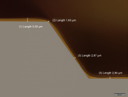
Fig. 5c Section of a resist-coated etch pit, the resist layer is noticeably thinner at the upper edge 5c)
Dip coating is mainly used in optical industries to e.g. coat rectangular, up to 4 m long glass substrates with resist (Fig. 6). The substrates are immersed in a large resist bath and then carefully moved up with defined pulling rates using a lifting device. The accuracy of the layer thickness can reach up to + 5 nm for the 4 m substrates. Also irregularly shaped or conical substrates can easily be coated with this procedure.
Felt coating is a special form of coating. A felt sheet which is steadily loaded with resist is pressed onto a 2 cm-wide metal strip for linear encoders that can extend up to several kilometres. The metal strip rotates under the resist-loaded felt at constant speed, thus coating the long strip successively (Fig. 7).

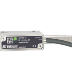
Fig. 6 High-precision incremental scale, produced by dip coating 6)

Fig. 7 Exposed linear encoding system, visible in the background is a part of the structured metal strip 7)
Roller coating was in the 90s for a long time particular relevant for the production of printing plates. Aluminium plates with dimensions of up to 1 x 1 m were pushed under a roller which was continuously supplied with resist from a storage container (Fig. 8). After the printing technology changed more and more towards digital processes, printing plates are rarely required anymore. Roller coating is still used for large substrates, e.g. for the coating of large solar cells or the roll-to-roll process of nanoimprinting.

Fig. 8 Structure of a roller coating device 8)
Resist coatings can also be realised via inkjet technology. The resist is dispensed over the entire surface of complicated (even irregularly shaped) substrates, exposed and structured, but inkjet printers are also able to reproduce rougher structures from digital images themselves.
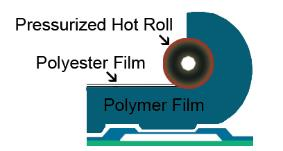
So far, exclusively substrate coating with liquid resists has been described. For the coating of printed circuit boards with a market share of to date 30 %, basically exclusively dry films [18] are used, except from a few special microelectronics applications, e.g. as protective layers. Solid resists are offered as films (Fig. 9a) that are laminated onto circuit boards and thermally adhered to the substrate (so to speak, ironed-on, Fig. 9b). Only weakly alkaline solutions are required as developer, which is environmentally friendly. A further advantage is that basically the entire material is utilisable, due to only minor losses during the coating procedure (in comparison: during spin coating, 95 % of the resist is wasted). However, a certain film thickness is required for mechanical stability. With a usual layer thickness of 50 µm, resolutions of only up to 25 µm can be achieved; special films with a thickness of 5 µm allow for a resolution of up to 5 µm [19].

Fig. 9a General build-up of dry resists. The structurable polymer film is in the middle of the three layers9a)

Fig. 9b A heated roll presses the polymer film onto the circuit board 9b)
3.3. Softbake:
Quite often solvents residues are still present in the layer after spin coating which can be expelled at temperatures around 100 °C with a softbake. The coated wafer is thereafter easily processable and does not adhere e.g. during contact exposure. A softbake is also highly recommended for other general resist properties on the wafer. A comparing of two wafers which were either annealed at 95 °C or dried at room temperature overnight (which is in principle possible) shows that the layer dried at room temperature is formally 8-times more sensitive, but the dark erosion (see 5.1.1.) is in this case 10-fold higher and the entire resist layer would thus completely disappear within a few seconds. For a precise process flow, temperature and time must be strictly controlled. Two methods are generally used for the softbake: The hotplate is a round heating plate with precisely adjustable temperature which removes the wafers immediately after tempering (Fig. 10). The second method is a convection oven drying up to 25 wafers at once (Fig. 11). Typical heating times on a hot plate are 1 – 2 minutes for layer thicknesses of up to 5 µm; the drying process in the oven takes about 25 – 30 minutes. For very high layer thicknesses of up to several hundred µm, a softbake may well require a few hours. Available are also special hotplates that use NIR radiation for drying in addition.

Fig. 10 Hotplate, EV Group10)

Fig. 11 Vacuum convection oven, Gallenkamp 11)
3.4. Positioning:
Important is that the desired structures are precisely placed on the wafer. For the manufacture of a circuit, many successive sub-steps must be carried out in exactly the same spot, which is why wafers have to be positioned within an accuracy of a few nanometres.
3.5. Irradiation:
During irradiation, the exposed parts of a resist film are chemically changed and become soluble in the case of positive resists, while negative resists are rendered insoluble upon irradiation (see section 4).
For the fabrication of specific structures, lithographic photomasks are used. Photomasks (reticles) are high-precision, mostly square opaque plates covered with a thin chrome layer into which the desired patterns are incorporated. Simpler patterns are produced by photolithography; more precise structures require electron beam lithography. The production of the often highly complex masks suitable for the deep UV range with several dozen process steps can easily cost some ten thousands of euros per mask.
The various lithography processes depending on the respective wavelength are outlined in section 4. Here, we firstly describe exposure methods and exposure devices for the optical lithography. Probably the most frequently used device is a mask aligner (Fig 12) transmitting light of certain wavelengths which is in most cases further selected by filters. The light waves are bundled via optical systems and directed through a photomask with the structures to be transferred onto the wafer, and the entire resist layer is exposed in one step. Two methods are used for this purpose: The highest resolution can be achieved with contact exposure in which the mask is pressed directly onto the wafer. However, the direct contact always involves the risk that the mask will stick to the wafer due to insufficient drying. With proximity exposure, mask and wafer are separated by a gap of 10 – 50 µm. A soiling is thus excluded, but the resolution is decreased.

Fig. 12 Mask Aligner EVG 610, EVGroup 12)
Exposure steppers in contrast transfer a (usually fivefold) reduced-scale image stepwise by projection exposure to the resist layer on the wafer. This reduction also minimises the reproduction of particles that maybe present on the mask and thus almost completely prevent interference. In addition, production of the masks is easier and cheaper, due to the coarser structures. The individual images are transferred using a “step and repeat” process, whereby the wafers are moved and positioned using extremely precise mechanisms (e.g. apiezo linear drive). Due to the finite depth of field of the imaging optics, only thin photoresists can be exposed with this method, while contact and proximity exposure also allows for lithography in thick photoresists [20]. In comparison, the mask aligner is the faster procedure because the entire wafer is exposed at once.
Optical lithography can also be used for structuring without masks. In direct laser writing (direct laser lithography), a laser beam of a specific wavelength (typically 405, 363 or 351 nm) is guided horizontally over the substrate at a speed of up to 240 m/s. During the scanning movement, the laser beam is switched on or off in fractions of a second. The vertical movement of the exposure material (feed) during the scan leads to line-by-line image formation of the exposure area. Suitable as laser source are UV LEDs, semiconductor lasers, frequency-multiplied solid-state lasers or excimer lasers. Direct laser exposure is the most commonly used exposure method in circuit board industry. To reduce the writing times, meanwhile devices are available that operate with more 200 laser beams in parallel. High-quality direct writers are also used in microelectronics and optical industry. Here, it was even possible to optimize the laser beam for structures down to the sub-µm range [21]. Since the method does not require complex and costly masks, it is particularly well suited for prototyping and the exposure of spherical substrates.
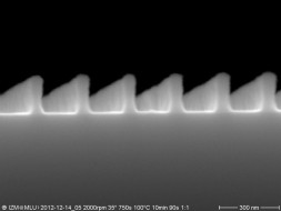
Interference lithography is a rather rarely used method for patterning. The principle is the same as in interferometry [22, 23] or in holography [24]. The superimposition of two or more coherent light waves leads to the formation of a periodic interference pattern which consists of a series of intensity maxima and minima (superimposition or extinction) and can be recorded in light-sensitive layers (photoresists) (Fig. 13 and 14). This process can even be used for films with a thickness of up to 100 µm [25]. Suitable resists are e.g. SU-8, AZ 9260 or CAR 44.

Fig. 13 Principle of interference lithography 13)

Fig 14 Interference structures with AR-P 3840 14)
Two-Photon Polymerization (2PP) enables a three-dimensional structuring of any complex models with a resolution in the sub-µm range (Fig. 15 and 16). The structuring process is based on the principle of direct laser writing which uses the non-linear two-photon absorption in the focal point of a tightly focused femtosecond laser beam. A polymerization reaction restricted to the focal volume is induced which solidifies a transparent photosensitive material. Originally, three-dimensional structures were produced from a liquid mixture of photoreactive monomers by selective cross-linking [26 – 29]. Meanwhile it is however also possible to use solid layers of negative resists like SU-8, Atlas 46 of ORMOCERE (section 7.5) for the fabrication of such structures.


Fig. 15 and 16 Examples for complex structures fabricated with 2PP lithography 15), 16)
3.6. Post-Exposure Bake (PEB):
This optional bake step is used to promote additional chemical reactions or the diffusion of components within the resist layer.
3.7. Development:
During development, those areas of the resist which have become soluble upon exposure (positive resists) or areas soluble from the start (negative resists) are completely dissolved by the developer and only the desired (insoluble) structures remain. The optimal result of the development depends on the concentration of the respective developer and the development time, and both parameters must be precisely maintained. Three methods for development are commonly used: For immersion development, single wafers or cassettes containing several wafers are immersed in a developer bath, mechanically agitated, quickly removed from the bath and rinsed after the time has elapsed. For puddle development, the wafer is placed on a spin coater and a defined amount of the developer is deposited on top of the wafer. The wafer rotates gently back and forth in half-second intervals, the developer is then quickly spun off and the wafer rinsed with water. For spray development, the wafer is likewise placed on a spin coater and the developer solution is applied onto the wafer at moderate spin speeds using a spray nozzle. At the end of the development, the wafer is rinsed with water at higher spin speeds.
The majority of photoresists and many e-beam resists are developed with aqueous-alkaline developers which either contain metal ions or are metal ion-free (MIF). Metal ions interfere with many semiconductor processes; they modify the properties if e.g. a subsequent plasma etching step after development is intended. Metal ions (mainly sodium or potassium) are incorporated into the semiconductor material and change the microelectronic properties. For this reason, preferably MIF developers based on TMAH (tetramethylammonium hydroxide) are used. These developers are fast and aggressive, which is generally beneficial for the efficiency of the process. If however a higher contrast and/or resolution is aimed at or if very thick resist films are developed, developers containing sodium hydroxide, potassium hydroxide, phosphates or borates are often favoured.
Based on their specific chemical structure, many resists require developers containing organic solvents, i.e. negative resists SU-8 and Atlas 46 in photolithography and all PMMA resists as well as ZEP 520 and CSAR 62 in e-beam lithography. In contrast to aqueous-alkaline developable resists, the polymers of these resists possess no OH groups. After cross-linking (negative resists) or cleavage of the molecules (positive resists), organic solvent mixtures must be used to carve out the structures (see also section 4.1.5.). Development is usually completed after 1 – 2 minutes, may however take more than 10 hours for extremely thick PMMA layers more than 1,000 µm as used in LIGA processes (see section 4.1.8.).
3.8. Measurement and Inspection:
With this optional step it is possible to check after development if the created structures meet the desired quality requirements. In some cases, errors can still be corrected; in the worst case, the wafer has to be discarded.
3.9. Hard Bake:
Another optional step is the hard bake. Particularly if resist structures are in the following subjected to ion implantation or plasma etching, a hard bake increases the stability of the structures and the expulsion of volatile components (solvents). Both aforementioned techniques require high vacuum conditions which are impaired by volatile substances.
3.10. Technological Steps:
The processed wafer can thereafter be subjected to further processes such as doping, implantation, plasma etching, vapour deposition of metal or an etching of the wafer. These customer-specific steps are only marginally related to the actual imaging process and thus not described here.
3.11. Resist Removal (Stripping):
Resist structures no longer required are in most cases removed at the end of the lithography process, unless (in rare cases) they do not interfere with subsequent steps. The resist structures themselves are only used for a few applications, e.g. in microfluidics [30] when micro-channels or chemical mini reactors (reaction volume < 1 ml) are fabricated from the resist. Several organic solvents or strong aqueous-alkaline solutions are available for removal. If resists were processed according to standard conditions, the removal generally poses no problem and can in many cases even be achieved with acetone. But if resist structures were previously exposed to high temperatures (> 180 °C), intensive plasma etching processes or high-temperature implantations, stripping may be difficult or almost impossible. In this case, removers that can be heated up to 80 °C (e.g. N-ethyl-2-pyrrolidone, AR 300-72) might work, possibly with additional support by ultrasound treatment. Otherwise, only intensive oxygen plasma remains as final solution to remove the unwanted resists.
4. Advanced Lithographic Patterning Techniques
Photolithography is the most important technique for the fabrication of microstructures and utilises photo- and radiochemical imaging methods. Apart from this, three other methods exist that are not primarily based on a direct structuring with light: Thermal scanning probe nanolithography, block copolymer self-assembly imaging method and imprint imaging. For the sake of completeness, these methods are briefly described at the end of this section.
- Optical lithography, extreme UV lithography, electron beam lithography, ion beam lithography
- Thermal scanning probe (nano-)lithography (t-SPL)
- Block copolymer self-assembly lithographic imaging
- Imprint imaging
4.1. Optical Lithography
This process was developed about 50 years ago and created the preconditions for all further developments in microelectronics. The optical lithography of the first generation (UV broadband 300 – 450 nm wavelength) is still used essentially unchanged in industry today. Microchips produced with this technique make up a major part of the current market volume.
The following equipment is required for optical lithography: 1.) A radiation source, generating light of the required wavelength. 2.) An optical system, focusing the light via a photomask (reticle) on the wafer. 3.) A photomask with the desired structures. 4.) An optical projection system, transferring the image onto the resist when the light passes through the mask. 5.) A wafer holder, placing the wafer in the correct position. 6.) A photoresist-coated wafer.

Fig. 17 General set-up for optical lithography 17)
The optical lithography uses light for the lithographic process; in this case the part of the entire electromagnetic spectrum ranging from 436 nm to 126 nm wavelengths (see Fig. 18).
To optimise the performance of microchips, one goal is to increase the integration density of the circuits by producing ever smaller structures. The size of the structures that can be realized also depends on the exposure wavelength; the shorter the wavelength of the light, the higher the resolution. Due to technical reasons, the first generation optical lithography used broadband UV with the typical wavelengths of 435 nm (g-line), 405 nm (h-line) and 365 nm (i-line) of the Hg spectrum (see Fig. 18). In the course of the further development, devices and resists emerged that could use the short-wave range down to 126 nm.
4.1.1. Broadband UV, g-line (435 nm), h-line (405 nm), and i-line (365 nm) Lithography
The designations g-, h- and i-line are derived from the emission spectrum of high-pressure mercury (Hg) lamps (Fig. 18).

Fig. 18 Radiation spectrum used for lithographic applications 18)
Broadband UV wavelengths are applied for the exposure of many different resists, most commonly positive resists based on naphthoquinonediazides or novolaks. But also some other resists (positive, negative, image reversal, chemically amplified or not chemically amplified) for special applications are exposed to broadband UV. Broadband UV lithography is thus the imaging technology with the greatest variety of applicable resist and processes. The highest resolution achieved with this lithography process is currently in a range of 0.25 µm.
4.1.2. KrF (248 nm) Lithography
KrF lithography is mainly characterised by the use of a powerful krypton fluoride (KrF) exciplex (excimer) laser [31, 32]. Due to their specific absorption properties, resists suitable for this technology are mostly chemically enhanced poly(hydroxystyrenes) with highest absorption (i.e. sensitivity) at a wavelength of 248 nm. Meanwhile, resolutions of 0.13 µm can be achieved with this technology.
4.1.3. Dry- and Water Immersion ArF (193 nm) Lithography
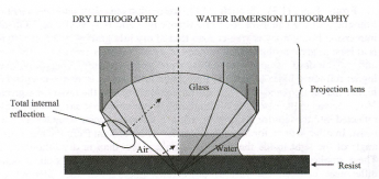
If argon fluoride (ArF) excimer (exciplex) lasers with a wavelength of 193 nm are used for irradiation, the resolution can be improved down to 65 nm (0.065 µm). Resists suitable for such applications are chemically reinforced and based on polyacrylates, polycycloolefins and polycycloolefin/maleic anhydrides. Two different methods are currently applied for this purpose; one method uses air between the last lens and the resist layer (dry lithography), the other method uses water instead (water immersion lithography) (Fig. 19). Due to the improved optical properties (i.e. the refractive index), water allows for a greater depth of contrast [33].

Fig. 19 Principle of dry and water immersion lithography 19)
In current technologies, also the wavelengths of 157 nm and 126 nm of excimer lasers are utilised.
4.1.4. Extreme Ultraviolet Lithography (EUV)
EUV lithography utilises the wavelength of 13.5 nm for the exposure of resist layers. To achieve a high-resolution patterning of periodic structures, the (achromatic) Talbot lithography is ideally suited for partially coherent radiation with a defined bandwidth, as is provided by a plasma-based radiation source [34, 35]. Fig. 20 shows a simplified diagram of a typical EUV system [36 – 38]. Resist primarily used for this purpose are e.g. SERV 140 and JSR3030. The maximum achievable resolution is approximately 15 nm.

Fig. 20 Schematic set-up of a EUV device 20)

Fig. 21 Principle of the Talbot lithography 21)
4.1.5. Electron beam lithography
In electron beam lithography, highly focused electron beams are used for exposure and structuring. The wavelength of the electrons is in a range between 0.012 and 0.024 nm (50 kV to 100 kV), depending on the acceleration voltage. Resolutions down to the nm range are thus generally possible [39, 40], but even an amazing resolution of 2.5 nm was already reported [41]. In the various resist films, electrons either increase the solubility as compared to the initial state (positive resist) or decrease it (negative resist). The chemical reactions are described in section 5.
The electrons are mostly generated by a tungsten emission source, then accelerated and focused by electrical fields (Fig. 22). In principle, two different writing methods exist: Point emitters scan the entire wafer with one electron beam which achieves a maximum resolution, but writing times can be extremely long and may take several days for a wafer. Shaped beam procedures use differently shaped masks (squares, triangles, circles etc.) which are placed in a fixed or variable width electron beam. The masks change in fractions of a second. In this way, “larger” areas (e.g. 50 x 50 nm) are irradiated with one shot which increases the writing speed considerably. Another option to shorten the process times is Mapper lithography [42, 43]. Dozens of electron beams write the same structures in parallel.
The big advantage of a maximum resolution is reduced by much slower process times in comparison to photolithography. E-beam lithography has thus only a relatively small market volume in microelectronics since the mass production of microchips is uneconomical. The major application field is the fabrication of photomasks for photolithography.

Fig. 22 Principle of electron beam devices 22)

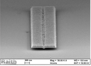
Fig. 23 Raith-Maschine 23)
4.1.6. Ion Beam Lithography
Ion beam lithography is similar to e-beam lithography in that the method itself and the equipment are identical, but the emitting source (ions instead of electrons) and the deflecting lens system differ. Since the energy of focused ions is higher than that of electrons, less sensitive resists can also be successfully used in ion beam lithography with acceptable writing times. Due to the high energy input, an even better resolution is possible [44, 45].
4.1.7. Synchrotron Lithography
In synchrotron lithography (deep X-ray lithography; LiGA = Lithographie, Galvanik, Abformung) [46], X-rays are used to irradiate and develop layers of up to 3 mm (e.g. PMMA). These structures are galvanically formed and used for the molding of another polymer (e.g. PDMS). The metal masks themselves can also be used, e.g. as gear wheels for high-quality watches. Since an extremely expensive synchrotron system is required for the process (e.g. CERN, Switzerland, Bessy, Berlin), the application is limited to relatively few users. Typical resists for the synchrotron are thick PMMA resists such as AR-P 6510 or the negative resists SU-8 and CAR 44. For extremely high layer thicknesses, PMMA sheets are used.

Fig. 24 Synchrotron Bessy II, Berlin Adlershof 24)

Fig. 25 Turbine wheel (50 µm thickness) for MEMS application with synchrotron exposure, resist CAR 44 AR-N 4400 25)
4.2. Thermal Scanning Probe Nanolithography
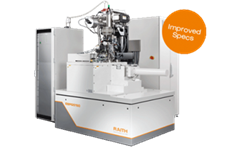
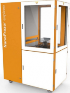
In the 1990s, first attempts were made to pattern resists residue-free with the hot tip of an atomic force microscope (AFM) [47, 48], which could indeed successfully be demonstrated for PMMA and polycarbonate polymers. The commercial application of this method however only became possible through the development of the NanoFrazor device and PPA (polyphthalaldehyde) resists [49, 50]. The decisive special feature of PPA resists is the possibility of dry development, i.e. their structuring can be performed without organic or aqueous-alkaline developer solutions. PPA is meta-stable at room temperature. When heated intensely, PPA breaks down into volatile components which are harmless to health. PPA layers can be structured either by direct laser writing or by thermal probe nanolithography; both processes exploit the thermal lability of the polymers. The PPA layer evaporates instantly upon heat input with a heated needle (NanoFrazor, SwissLitho) [51] or through the energy released during direct laser writing and is thus structured directly. So far, structures down to a resolution of 10 nm could be realised with the NanoFrazor. The commercially available PPA resist Phoenix 81 has a remarkably long-term stability for this class of resists [52].

Fig. 26a Three-dimensional image of Europe, produced with a hot needle 26a)

Fig. 26b NanoFrazor 26b)

Fig. 26c Chemical structure of polyphthalaldehyde and decomposition to monomers 26c)
4.3. Molecular self-assembly Lithography
Molecular self-assembly lithography is a rather new method. The technique is based on the spontaneous association of molecules under equilibrium conditions into stable, structurally well-defined aggregates that are connected by non-covalent bonds. The self-organizing precursor molecules react from a solution or the gas phase to form monomolecular layers. The chemical binding of these layers to solid surfaces occurs through thermodynamically favourable bond formation and chemisorption. Such polymers belong to a class of materials called self-assembling monolayers (SAMs) and can be used as ultra-thin resists. The molecular structure of SAM resists differs, thus allowing for different lithography processes for structuring, e.g. electron and ion beam, deep UV or synchrotron lithography [53 – 55]. With electron beams, already structures of 20 nm could be achieved [56]. Fig. 27 exemplarily shows the fabrication of a block copolymer (BCP) self-organizing layer (for an overview, see reference [57]. In comparison to other methods, the industrial use of SAMs is still in its early stages [54, 58, 59].

Fig. 27 Approaches for lithographically directed self-assembly (DSA) of block copolymers (BCP). Graphoepitaxy, in which topographical patterns are lithographically transferred in a substrate to control the directional self-assembly (DSA) of the block copolymers (left). Chemoepitaxy, in which lithographically generated chemical patterns are used to direct the DSA of the block copolymers (right) 27)
4.4. Imprint Lithography
Imprint lithography is not an imaging process in the sense of the techniques presented so far since the (micro) structures are in this case not created by photons, but by imprinting [59, 60]. The structures are pressed into a thermoplastic or photo-cross-linkable thin polymer layer via inversed stamps (masters). The stamps themselves are produced with photo or e-beam lithography. Structures can then be cured in two ways: The shaped layers with the stamp are heated, the polymer layers cross-link and the stamp is thereafter removed. The second method cross-links the formed layers using a stamp that is transparent to UV radiation, followed by flood exposure. Both procedures are shown in Fig. 28.

Fig. 28 Imprint lithography procedures 28)

Fig. 29 Roll-to-roll procedure 29)
Soft lithography is a modification of imprint lithography and uses elastomers like PDMS (polydimethylsiloxane) for the replication of structures. The PDMS stamp which provides a particularly high resolution is produced with photoresist structures. Roll-to-roll (R2R) photoimprint lithography (R2R-PIL) enables a large-scale production of microstructures. At first, the structures of the master are applied onto a roller, followed by application of the imprint resist to a flexible film and the structuring by the master (Fig. 29). The structures are then applied to another film. With this method, structures down to a few 10 nm can be realised. The industrial use of very different applications has increased enormously in recent years so that numerous imprint resists are commercially available. Larger users of imprint technology partly produce their resists themselves.
5. Resist Chemistry
5.1. Positive Resists
The general process steps for positive resists are described in section 3.
5.1.1. Naphthoquinone Diazide (NCD)
The probably best known and most frequently used system is the NCD/novolak photoresist. In 1940, Oskar Sues developed the reaction later named after him which is, so to speak, the “mother“ of all photolithography reactions. Upon irradiation, the diazo group is split off from NCD (-N2). After addition of water, an unstable intermediate (ketene) results which further reacts to indene carboxylic acid.

Fig. 30 Sues reaction of naphthoquinone diazide to indene carboxylic acid 30)

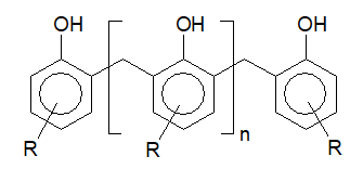
Fig. 31 Structure of novolak 31)
Positive photoresists mainly consist of NCD, novolak and solvents [61]. Due to the OH groups of the polymer, pure novolak layers are easily soluble in aqueous alkaline solutions (developers). An important parameter for photolithography is the alkaline dissolution rate or ADR, which is the speed at which a novolak layer dissolves in a defined strong developer in nm/s. Upon addition of NCD to the novolak, the ADR drops by a factor of more than 100 (Fig. 33) due to the interaction of NCD with the OH groups. The OH groups of novolaks are for example blocked by van der Waals bonds, so that the alkaline dissolution of the novolak is inhibited (Fig. 32). If novolak/NCD layers are exposed, the Sues reaction is initiated and alkali-soluble indene carboxylic acids are formed. Together with the newly exposed OH groups of the novolaks, the alkali solubility increases by a factor of 10 as compared to a pure novolak layer (Fig. 33).

Fig. 32 Blocking of OH groups (inhibiting effect) by NCDs (left) or sulfone groups (right) 32)

Fig. 33 Schematic diagram of dissolution rates 33)

Fig. 34 Dissolution rates depending on the NCD concentration 34)
The difference in the dissolution rate between the exposed versus unexposed novolak/NCD (photoresist) layer is thus > 1,000, i.e. unexposed areas are not attacked (no dark erosion). Fig. 34 shows how the NCD content in a resist influences the solubility rate. Experience has shown that the optimal concentration is in the range of 20 – 25 % NCD (solids content). A lower concentration causes increased dark erosion, a higher concentration renders the resist too insensitive.
A further important resist parameter is the contrast (gradation). To determine the contrast, a resist is coated onto a substrate and the layer thickness is measured. Then an exposure series with different doses (exposure level) is applied and developed with an aqueous alkaline developer. Depending on the dose, still underexposed areas are not attacked. With increasing dose, more and more is removed from the resist until it is completely developed. The different layer thicknesses are measured and plotted against the decimal logarithm (Fig. 35). A tangent is applied to the curve; the derived slope yields the contrast.


Fig. 35 Gradation curve of a positive resists and corresponding formula 35)
If a marginal increase of the exposure level (e.g. from 50 to 52 mJ/cm²) is sufficient to develop the entire layer, the contrast is high. A high contrast is necessary to achieve a maximum resolution (vertical walls of resist structures). However, if three-dimensional “analogue” structures are desired (Fig. 51c), a low contrast should be chosen. The contrast depends on both the resist composition and the development conditions. This behaviour with respect to the contrast applies to all resists, only that the curve shown above (Fig. 35) runs in the opposite direction for negative resists. Negative layers cross-link upon irradiation and built up to the initial layer thickness with increasing exposure dose.
A special development are image reversal resists which are positive resists containing an amine component. If this resist layer is exposed image-wise, annealed (cross-linking reaction between exposed NCD, amine and novolak) and subsequently flood exposed (exposure of the previously unexposed areas), a negative structure results [62].
A small selection of typical resists: AZ series (AZ Electronics), MicroPosit S 1800 (DOW), TFR series (Tokyo Ohka Kogyo), AR-P 3500 series (Allresist)
5.1.2. Chemically enhanced positive Resists (CAR) for optical Lithography
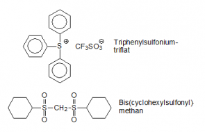
Chemically amplified positive resists come in a large variety of different formulations, but the principle is always the same [63]: An aqueous-alkaline soluble polymer due to its OH groups such as poly(hydroxystyrene) becomes alkali-insoluble after chemical addition of protective groups (tert-butyloxycarbonyl, t-BOC) at the OH groups. If the polymer is dissolved in an organic solvent and a strong photo acid generator (PAG; Fig. 36) is added, a chemically amplified resist is obtained. Upon exposure (the required wavelength depends on the respective PAG; UV to electron beam is possible), the protective groups are split off by the newly formed protons and the exposed resist can be developed again in aqueous-alkaline solutions (Fig. 37). Since the PAG has a catalytic effect, one proton is able to remove a large number of protective groups. Chemically amplified resists are thus much more sensitive than non-chemically amplified resists. The acids however tend to diffuse in the layer which significantly decreases the resolution.
A small selection of typical resists: Apex E, UV6 (Dow), Arch 2 (Arch), APEX – E, AZ PF 514 A (Hoechst), EOS 72 (Allresist).

Fig. 36 Acid generators for chemically enhanced resists 36)

Fig. 37 The protected polymer is deprotected by protons (H+) 37)

Fig. 38 Tert-BOC poly(hydroxystyrene) is converted into poly(hydroxystyrene)38)
5.1.3. Positive Resists for Electron Beam Lithography
The first electron beam devices were produced at the end of the 1970s. The first resists consisted of poly(methyl methacrylate) (PMMA) and are still widely used today because PMMA resists are extremely reliable, versatile, and easy to handle. The principle of action is based on the cleavage of the molecular chain. Generally used PMMAs have a molar mass between 50,000 g/mol (50 k) and 950,000 g/mol (950 k). If the long-chain molecules are irradiated with electrons, the main chain is cleaved in many places. The resulting fragments of < 5,000 g/mol are readily soluble in special solvent developers, while the unexposed high molecular weight polymers remain insoluble. With PMMA resists, resolutions down to 5 nm can be achieved. If a PMMA copolymer with methacrylic acid is used, the sensitivity can be increased by a factor of 3. Due to its aliphatic structure, PMMA is however relatively susceptible to plasma etching processes. For this reason, positive e-beam resists like ZEP 520 and CSAR 62 are better suited for such applications. Both are copolymers of chloroacrylates (to increase the sensitivity) and styrenes (to improve the plasma etching stability). With CSAR 62, a resolution of 8 nm with a layer thickness of 180 nm could be demonstrated [64]. As already mentioned in section 5.1.2, chemically amplified positive resists are also used for e-beam lithography (FEP 171). The chemical structure and mode of action are similar to the resists described here.
Novolak-based positive photoresists take a special position; they are primarily used as positive e-beam resist for mask production. Particularly interesting is the chemical reaction (see section 5.2.2).
A small selection of typical resists: PMMA 50 k to 950 k (MCC, Allresist), ZEP 520 (Zeon), CSAR 62, AR-P 617 PMMA copolymer (Allresist), FEP 171 (Fujifilm), AZ series (AZ Electronics).
5.2. Negative Resists
The process steps for negative resists are described in section 3.
5.2.1. Negative Resists for Photolithography
The Kodak KTFR poly(cis-isoprene) negative resist was the first photoresist applied in mass production from 1957 onwards. The achievable resolution was 10 µm, and the resist had to be developed with environmentally hazardous organic solvents. It is basically no longer used today.

Fig. 39 Upon exposure, N2 is split off from the bisazide. Radicals are formed which react with polyisoprene and cross-link the compound 39)
In the 1990s, new negative resists were developed. The well-known negative resist SU-8 of the company Shell consists of an epoxy resin plus photo acid generator (triarylsulfonium hexafluoroantimonate) dissolved in organic solvents (cyclopentanone). Upon exposure, a strong acid is formed which induces multiple cross-linking. SU-8 is highly sensitive and the structures are extremely stable, but a removal is difficult and requires a complex process. Meanwhile other resists (Atlas 46) based on epoxy resins with similar properties are available. The variant Atlas 46 R (“R” for removal) can be removed comparably easily. Epoxy resists are usually developed with organic solvents.

Fig. 40 Structure of the epoxy resin SU-8 and appropriate acid generator 40)
As further improvement, also an epoxy resin resist (KMPR) is available that can be developed aqueous-alkaline. In photolithography, the three last-mentioned resists can be used to produce structures up to a layer thickness of a few hundred micrometers. If synchrotron radiation is used, even structural heights of more than 1 mm (> 1,000 µm) are feasible. The negative resists are completed by CAR 44 which consists of novolak (like positive resists), an aminic cross-linker and a PAG. This resist is environmentally friendly, easily removable and can also be exposed at g-line (436 nm).
A small selection of typical resists: KTFR (Kodak), SU-8, KMPR (MCC), Atlas 46, CAR 44 (Allresist)
5.2.2. Negative Resists for Electron Beam Lithography
Photoresists such as AZ 1518 or IP3500 are widely used, especially in mask manufacture, and can be applied as negative or as positive electron beam resist (section 5.1.3). The reason for this is to be found in the particular reaction mode of NCD (section 5.1.1, Fig. 30). For positive processes, water is required to form indene carboxylic acid. Surprisingly, even in the high vacuum of the e-beam lithographic system (up to 10-9 Torr), a sufficiently high amount of water is available to allow for the Sues reaction to take place; consequently a positive image is created. At higher bake temperatures of the resist and higher exposure doses, unstable radical ketenes (Fig. 30) are formed during irradiation that react with novolak and induce cross-linking. This creates a negative image, but the sensitivity is greatly reduced.
Also negative e-beam resists can be chemically amplified (CAR) or non-chemically amplified (non-CAR) resists. A non-CAR is the AR-P 7520 composed of novolak and a bisazide. Upon irradiation of the bisazide, nitrogen is split off and the resulting radical cross-links the novolak (Fig. 41).

Fig. 41 Cross-linking reaction: bisazide and novolak before and after cross-linking 41)
Since no PAGs diffuse in the layer (as is the case with CARs), high resolutions are possible (20 nm), but the sensitivity is also significantly lower due to the lack of chemical amplification. PMMA resists are normally positive-working (see 5.1.3.). If the radiation dose is increased by a factor of 50, a negative-working resist results. The high number of electrons generates a large number of radicals which cross-link and reverse the positive effect. This is however associated with long writing times. Chemically amplified negative resist (SAL 605, AZ nLof) contain aqueous-alkaline soluble polymers, and the addition of PAGs makes them sensitive to radiation. When exposed, they cross-link with high sensitivity and can be developed negatively. The maximum resolution is almost 100 nm.
Both SU-8 and Atlas 46 can be used as electron beam resists with high sensitivity, but in both cases, layers are difficult to remove after exposure. The electron beam resist HSQ based on hydrogen silsesquioxane polymers creates negative structures that are known for their high resolutions (2.5 nm) and high etch stability. The low sensitivity and process instability are however disadvantageous. Now a more sensitive and more process-stable alternative is available, Medusa 82. Due to its similar (but modified) chemical structure, the sensitivity could be increased by a factor of 20 while the high resolution is maintained.
A small selection of typical resists: KTFR (Kodak), SU-8, KMPR (MCC), Atlas 46, CAR 44, Medusa 82 (Allresist)
6. Further Resists for special Applications
Resists and process chemicals described so far are supplemented by a variety of other resists for special applications. In the following, some of the resists probably most interesting for users are presented.
6.1. Conductive Coatings
Conductive coatings are especially required in electron beam lithography. When electrons write structures on insulating substrates (GaAs, quartz, polymer; see also 4.1.5.), the substrates are electrostatically charged. Due to the insulating properties, these charges cannot be dissipated and deflect the beam uncontrollably during the scanning of the wafer. Consequently, the structures are distorted.

Fig. 42 Charging of an insulating substrate


Fig. 43 Structure without dissipation of charges (left) (e.g. quarts) by electron beams 42) and with the use of conductive materials (right) 43)
One solution is to vapour-coat the resist with a 10 nm-thin gold layer deriving the charges. After extensive vapour deposition, the gold must however be removed before development. A more elegant solution is to apply a conductive organic layer by spin coating. Currently, two conductive resists are commercially available for this purpose: Espacer, (Showa Denko) and Electra 92 (Allresist). Both resists are water-based and can thus be spun onto the electron beam resist without dissolution. After irradiation, they are simply removed with water. Electra 92 is characterized by a particular long-term stability. Another application is the replacement of metal vapour deposition in scanning electron microscope (SEM) images. Also in this case the organic layers discharge the electrical charges and high-contrast images are generated. Since these conductive layers can be removed with water, the substrates can be used further.
6.2. Anti-reflective Coatings
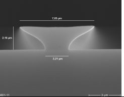
Undesired reflections on the substrate negatively influence the exposure process. If wafers have e.g. deep-etched silicon trenches (Fig. 5b), the light is reflected between the sidewalls of the trenches, thus causing defective structures. Coloured resists can be helpful; the scatter radiation is minimised due to an increased absorption of the dyes with absorption maxima at the exposure wavelength [AZ dyed, AR-P 3840]. Reflections on flat substrates have even more serious effects. During monochromatic exposure, e.g. i-line 365 nm, the incident light hits the glossy wafer surface and is reflected vertically upwards, perpendicular to the incoming light travelling to the substrate. Depending on the phase shift, light waves are either extinguished or amplified (Fig. 44).

Fig. 44 Schematic drawing of amplification and extinction 44)

Fig. 45 Resist structure with pronounced “standing wave effect“ 45)
The resulting resist lines then show an inhomogeneous, wave-like pattern (Fig. 45). This undesired effect can be largely eliminated with a post exposure bake. If the resist is irradiated with two or more wavelengths (UV broadband), the effect does not occur because the interference patterns mix. For short-wave exposure (see sections 4.1.2. – 4.1.4.), mostly monochromatic light is used and anti-reflective coatings are thus highly recommended. Anti-reflective coatings can be placed under the imaging resist (BARC bottom) or on top (TARC top). Bottom resists are either organic polymers that contain a dye with an extremely high absorption coefficient or inorganic sputtered-on layers with precisely defined layer thickness. Both extinguish the incident light almost completely. The TARC top resists should not dissolve the respective resist layer during the coating and must have a refractive index of approximately 1.28. These requirements are met by perfluorinated polymers and solvents. Typical resists are e.g. AZ BARLi and AZ Aquatar.
6.3. Protective Coatings
In the course of the numerous process steps during the manufacture of ICs, the already created sensitive structures sometimes have to be protected in subsequent process steps, e.g. simply for a transport to the next production facility. In this case, a not photosensitive coating (mostly novolak-based) is spun on which protect the structures during transport. The layer can then easily be removed again. Such coatings (AZ 520D, SX AR-PC 5000/3.1) also resist acidic media up to pH 1 (but no oxidizing acids) and dilute hydrofluoric acid mixtures (HF). The PMMA-based coating AR-PC 503 or the hydrocarbon-based Black-Protect (AR-PC 5000/41) can be used for full-surface protection against strong HF solutions or strongly alkaline KOH etchers. 40 % KOH is used to etch pits in silicon wafers (see Fig. 5b). No resist structures survive an etching process lasting several hours; in this case, a hard mask is required. For this purpose, silicon oxide is sputtered on the silicon and structured with a photoresist. The resulting hard mask can now be used for silicon etching. The oxide is then removed again.
6.4. High-temperature Resists
Some applications in microelectronics or microsystems technology require resists that withstand temperatures of up to 400 °C without destruction. Two examples are wafer bonding in which two wafers are connected, or soldering processes. Several products like BCB resists (benzocyclobutene, Sigma Aldrich) or polyimide resists (PHOTONEECE, Toray) are commercial available for high-temperature applications.
7. Technological Procedures
In the following, some special processes and procedures are presented that are directly related to the imaging process. This selection appears to be the most interesting for the author, and, again, it would be impossible to present all interesting and relevant areas here.
7.1. Lift-off Procedures
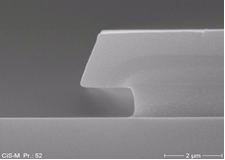
Conductor tracks are manufactured using either subtractive or additive processes. In subtractive processes, a metal layer which later yields the conductor track is vapour-deposited on the wafer, the resist then coated, exposed and developed. The exposed metal is subsequently etched away. After the coating structures have been removed, the desired conductor tracks remain. In additive processes, the resist is initially structured, the metal then evaporated and deposits on the resist structures and freely developed surfaces. Now the resist has to be removed to yield the remaining conductor tracks (lift-off). If resist flanks are however vertical or even positively inclined, the evaporated metal will completely cover the structures and the remover can no longer attack and remove the resist. The entire metallised layer remains. Therefore, undercut structures as shown in Fig. 46 are urgently required for the lift-off. Negative resists are particularly predestined for lift-off structures. If they are exposed to the full dose, they cross-link evenly strongly from top to bottom. However, if the dose is reduced, cross-linking occurs more pronounced at the top as compared to the bottom due to the inherent absorption of the resists at the exposure wavelength. In the subsequent development, the lower parts of the resist which are less cross-linked are more strongly attacked, resulting in an undercut (Fig. 46). If the metal is only evaporated onto the lower half of the resist layer, the remover has no difficulty in attacking and removing the exposed, upper resist.


Fig. 46 Differentially pronounced undercut of negative resists AR-N 4450. Shown in comparison are the results of higher (left) and lower (right) exposure dose 46)
7.2. Multi-layer Processes
Various multi-layer procedures are applied in microelectronics. The probably oldest two-layer system consists of two PMMA resists structured with e-beam lithography at the Academy of Sciences in Berlin in 1980. A low-molecular, more sensitive PMMA resist was used as bottom layer; a higher-molecular PMMA resist as the top layer. After irradiation and development, the bottom resist is attacked more strongly by the developer and an undercut is formed (Fig. 47) which can be used for lift-off processes (see section 7.1). With this method it is possible to vapour-deposit 20 nm-thin metal lines.

Fig. 47a Undercut structures of a PMMA bilayer after development 47a)

Fig. 47b Structures after evaporation of metal 47b)

Fig. 47c Metal lines after resist removal 47c)
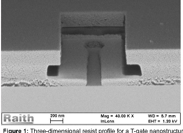
T-gates are required for the fabrication of acceleration sensors. These can e.g. be produced with high precision using the following e-beam three-layer system. The bottom layer is a PMMA resist (AR-P 672), the middle layer is the sensitive PMMA copolymer (AR-P 617), and the top layer is CSAR 62 (AR-P 6200). The centre of the structure is irradiated with a very high dose such that the bottom of the T-gate is written into the PMMA. The opening is subsequently irradiated with a medium dose so that the two upper layers can later be developed. Finally, the “side wings” are written with low energy into AR-P 617. The development then results in the desired resist structure (Fig. 49) which is filled with metal in a sputtering process. After removal of the resist structure, the desired T gate remains (Fig. 50).

Fig. 48 Schematic representation of the development process with two different developers 48)

Fig. 49 Resist structure of the three-component system 49)

Fig. 50 Final metal T-gate 50)
Multilayer processes are also used in photolithography, primarily to fabricate precise lift-off structures. A non-light-sensitive resist (PMGI, LOR or AR-BR 5400) serves as bottom resist onto which photoresists can be coated without being dissolved. After exposure, the photoresists are developed aqueous-alkaline and also the bottom resist is dissolved in this developer with a defined velocity.


Fig. 51 Two-component photoresist system (AR-P 3540/AR-BR 5460), different undercut due to different developing times. a) 25 s development, 0.8 µm undercut; b) 60 s, 2.0 µm; c) 120 s, 5.2 µm 51)
Figure 51 demonstrates that an undercut can be precisely adjusted via the duration of the development step. Such structures allow for a safe lift-off process.
7.3. Greyscale Lithography
The vast majority of microelectronic applications are concerned with the fabrication of digital structures, i.e. the generation of precise structures with ideally vertical flanks. However, also “analogue” structures are required in optical industry or in the production of holograms. For these purposes, three-dimensional resist structures are built up. This structure can be realized by exposing a suitable resist with different exposure energies (see Fig. 52a).

Fig. 52 a) Principle of greyscale lithography 52a)

Fig. 52 b) Diffractive optical element 52b)

Fig. 52 c) Hologram 52c)
The three-dimensional structures can be manufactured by photo- or e-beam lithography. Particularly elegant is the fabrication of DOEs (diffractive optical elements) with resist Medusa 82 since only one process step is required. The resulting analogue structures consist predominantly of SiO2 and thus have the same characteristics like quartz from which DOEs are otherwise produced in far more complex processes (Fig. 52b). A hologram produced from a 4 µm-thick PMMA layer is depicted in Fig. 52c.
7.4. Sand Carving
Resists are also used in applications which are rather unusual from the point of view of microelectronics. Sandblasting is used to clean or modify surfaces from substrates. If it is important to process only part of the surface, robust structures have to be applied to the substrates. These are mostly dry films, but liquid resists are also used for a few applications in microelectronics. It goes without saying that this process can’t be performed in a clean room [67].
7.5. ORMOCER® Hybrid Polymers for Microsystems Technology
Another example of the meanwhile highly diverse image structuring processes are ORMOCERs. These polymers are a mixture of organic and inorganic components and well suited to obtain structurable layers with defined electrical and optical properties. The structuring is preferably carried out by a selective polymerization reaction. In addition to other structuring processes, nanoimprint lithography and two-photon polymerization (2PP) in particular also allow complex three-dimensional shapes. The main application field is the fabrication of optical components [68 – 70].

Fig. 53 ORMOCERs are e.g. used in roll-to-roll procedures as thin dielectric print-on layer 53)
8. The international Resist Market
Resists are of indispensable importance for the industrial development. Microelectronics and many other associated industrial fields (see section 2) could not exist without resist research and production. In 1989, the liquid resists market volume totalled $ 460 million [71]. In 2019, the revenue was $ 5.3 billion [9], which is likely to increase to $ 6.8 billion in 2022. Analysts assume a steady annual increase of 5 to 8 % in the next decade. Dividing up the world market by resist production in thousand litres (2017 [9]), Japan ranks first (628), followed by North America (530), South Korea (490), Europe (228), China (185), and India (124). This order does not change when the consumption of resist per region is considered. In the long run, China is expected to have the highest growth rate in the consumption of resists, which is also in line with general economic forecasts. However, the global economy currently (2020) faces a period of transition. Due to the “America First” claim of the USA and the resulting distortions of the world market, certain regions, especially China and South Korea (conflict with Japan), will try to supply themselves independently with resists or to trade with reliable partners.
The resist market is a highly sensitive system since users are extremely dependent on a punctual and high quality delivery of resists. If the global players in microelectronics such as Infineon, Samsung or Globalfoundries are out of production for just one day, the economic damage may well amount to millions of euro. Manufacturers always have at least one second source, but any switch to a different resist is incredibly complex. This not only involves releasing the photolithography after quality management, but also all subsequent processes up to the finished product have to be adjusted. All in all, such a switch can take over half a year. If photolithographic processes run safely, no user will change the resist any more (“if ain’t broke, don’t fix it”) – which has considerable consequences in the marketing of resist sales. If a competitor sells a similar resist about 10 % cheaper, maybe a few very large manufacturers spending several million euros a year on resists will think about this offer. If a company offers resists for half the price, no one will believe in a sufficiently high quality of the products. There are actually only good chances for resist manufacturers to acquire new customers when new companies are founded, new technologies introduced, or when the previous supplier discontinues the supply of a certain product.
The market analysis conducted by ZION [9] confirms that resist manufacturers have better market chances if they are right from the start able to respond to customer’s wishes. Large resist suppliers accomplish this only to a limited extent, and mostly only with large customers. If users however need “just” 100 litres of special resist per year, large resist companies don’t want to and cannot meet the request due to their cost structures. Only Allresist GmbH offers customised resists for all its customers.
Relativising the previous statement it should however be added that this market concept primarily applies to strategically important resists. Process chemicals such as developers, thinners, removers or adhesion promoters from different suppliers are easier to replace and the replacement products can, after a certain test phase, be used for different resists. In this particular market, mutual price undercutting in fact plays a major role.
Reliable suppliers of raw materials for resists are of utmost importance for resist manufacturers. Since light-sensitive components and high-purity polymers or solvents are mostly produced for a manageable clientele of resist producers, generally not too many suppliers for special products exist worldwide. Until the 1990s, raw materials were mainly produced in Europe, but thereafter, the production gradually shifted to Asia. At the moment, Japan is still clearly leading, but China is becoming increasingly important in the resist market.
9. Global Resist Manufacturers
In 2017 [9], worldwide ten larger resist producers existed that operated supra-regionally. Even the number 10 of this market analysis, AZ Electronic Materials with a market share of 2.3 %, had an annual turnover of about US $ 100 million (total market in 2017: US $ 4.6 billion). The three largest manufacturers are Tokyo Ohka Kogyo (23.1 %), JSR Corporation (22.2 %) and Dow Chemicals Company (15.2 %) and maintain, just like the other major resist manufacturers, international production facilities. JSR Corporation and AZ Electronic Materials each produce in nine different countries, with AZ being the only company also represented in Germany. This explains the relatively high market share of China and India since both countries build up their resist production expertise in cooperation with the global players. Also medium-sized companies specialised in a few resist products operate on the market, e.g. Zeon Corporation (electron beam resists). A few smaller companies complete the resist market and cover the need for lower quantities of small microelectronics companies. EM Resist (England), Microchemicals (Germany), DisChem (USA) and micro resist technology (Germany) are SMEs mainly distributing products of larger resist manufacturers and a few own resist developments. Only the German company Allresist offers an almost complete product portfolio with self-developed and self-produced resists.
10. Environmental Aspects
All resist manufacturers are aware of the fact that they manufacture and sell chemical products with potential “hazardous substance” classification, and all are aware of the great responsibility towards their customers. When ethyl glycol acetate, which had previously been the main solvent for almost all resists with butyl acetate and xylene, was classified as teratogenic in the early 1990s, the resists worldwide were quickly switched to the safer solvent PMA (PGMEA). Halogenated hydrocarbons which had long been used in some resists due to their excellent drying properties are no longer found on the market today. The worldwide transport and the declaration of chemical products are subjected to strict regulations.


