PMMA resists are predominantly used for electron beam applications or as protective coatings in aggressive wet chemical etching processes. In principle, a structuring of a PMMA layer is also possible by means of deep UV exposure (220 – 266 nm). In this case however, there the sensitivity is low and long exposure times result.
This was the reason to look for a more sensitive PMMA variant. The principle of chemical amplification could successfully be transferred to PMMA polymers. The new special resist SX AR-N 4810/1 is a chemically amplified photoresist based on PMMA that can be developed anhydrously with organic solvents – a crucial property in the case of moisture-sensitive substrates. SX AR-N 4810/1 is offered as a solution in anisole.
Also thicker layers up to about 5 µm can be realized with this resist system (on request). Our developer X AR 300-74/3 is particularly well suited for the maximum layer thicknesses; the sensitivity is in the range of about 600 – 650 mJ/cm2 (broadband UV).
The new chemically amplified formulation is characterized by a very good sensitivity in the wavelength range of 300 – 410 nm. A g-line exposure (436 nm) is nevertheless still possible, albeit with significantly lower sensitivity.
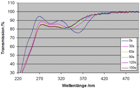
Fig. 1: Transmission spectrum; influence of increasing exposure time on the transmission (Hg vapor lamp)
With the new experimental sample SX AR-N 4810/1, resist thicknesses of up to about one micrometer are possible: ~ 650 nm (1000 rpm), ~ 480 nm (2000 rpm) and ~ 320 nm (4000 rpm). The developer consists of an ethylbenzene solvent mixture: X AR 300-74/1.
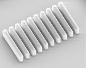
Fig. 2: Bar structure obtained with the new experimental sample SX AR-N 4810/1
The resulting structures are stable up to about 230 ° C and transparent in the optical wavelength range of >300 nm.
At the MLU Halle, SX AR-N 4810/1 was also investigated with respect to its suitability as resist for interference lithography. Since the LIL exposure was performed with only very low power (at 266 nm with ~ 0.3 mW/cm2), comparatively long exposure times are required:

Fig. 3: Bracketed series: LIL and broadband MJB-3 with SX AR-N 4810/1
While maximum layer thicknesses are already obtained after about 2 minutes of exposure to an Hg vapor lamp (broadband UV, ~ 10 mW/cm2), about 60 minutes are required in interference lithography for the same result.
The standard process allows the fabrication of well-defined resist architectures:
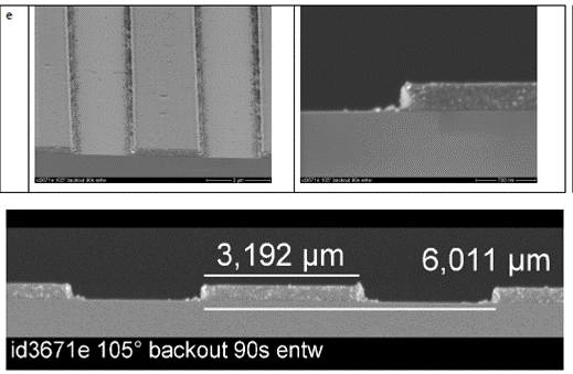
Fig. 4: Resist architectures with SX AR-N 4810/1
Optimal process parameters:
- 3 minutes exposure (broadband UV)
- 5 minutes PEB at 105 °C
- Development time: 135 s with X AR 300-74/1
Negative CAR PMMA resist SX AR-N 4810/1